SESSION OVERVIEW - INTERFACE CIRCUITS FOR IMAGERS
Click on one of the presentations below to read more:
 CMOS Image Sensors: Photons IN, Bits OUT
09:00
Albert Theuwissen
Harvest Imaging, Belgium Key circuits for single-slope analog-to-digital converters in image sensors
09:45
Guy Meynants
KU Leuven, Belgium Front-end Circuits for CMOS Single Photon Avalanche Diode Sensors
11:00
Robert Henderson
University of Edinburgh, United Kingdom SPAD-Based Flash LiDAR Sensors with In-pixel Histogramming TDC Architectures
11:45
Seong-Jin Kim
Sogang University, Republic of Korea Readout circuits for all-CMOS THz sensing and imaging
14:00
Matteo Perenzoni
Sony, Italy Noise Optimization of Micro-Bolometer Read-Out Ics
14:45
Sander Gierkink
Teledyne Dalsa, the Netherlands
PRESENTATIONS IN THIS SESSION
Albert Theuwissen
Harvest Imaging, Belgium
Abstract
To start, the participants will get a short introduction to CMOS image sensor (CIS) and to Single-Slope ADCs (SS-ADC). Because of the enormous parallelism in CIS, the SS-ADC is ideally suited to be used as a column-level ADC. Most of the presentation will focus on further fine-tuning of the ADCs knowing the noise behaviour of the CIS. Multi-slope and multi-ramp SS-ADCs are the result of this action. In this way speed and power consumption can be optimized. Other typical advantages of the SS-ADCs are the options to perform correlated multiple sampling (without any change in hardware) and auto-correction of non-linearities.
About the author
Albert Theuwissen got his MSc and PhD from KU Leuven (B) and after retiring from DALSA and Philips, he started in 2007 his own company Harvest Imaging. Harvest Imaging is focusing on training and coaching in the field of digital image capturing. In parallel to his industrial career, he also got a part-time assignment from the Delft University of Technology from 2002 till 2023.
Guy Meynants
KU Leuven, Belgium
Abstract
Single-slope ADCs (SS-ADC) for CMOS image sensors use a common sawtooth (ramp) reference signal coupled to a comparator for each column. The comparator controls a fast counter in each column that digitizes the signal. Challenges in the circuit design of this structure are discussed in this talk. The SS-ADC compares the pixel signal to the ramp signal twice per pixel sample to allow for digital correlated double sampling (CDS). A transient noise analysis of the comparator reveals that noise can be reduced when the ADC is clocked well above the comparator bandwidth. Kickback from the comparator onto the ramp signal should be avoided since it can cause visible artefacts in the image. Row noise can be avoided by operating with digital CDS during a single conversion cycle. Power dissipation and ADC conversion time can be optimized by the design and timing of the column counters.
About the author
Guy Meynants works on image sensors since 1994, first as a Ph.D. student at IMEC, and between 2000 and 2006 at IMEC spin-off FillFactory, acquired by Cypress Semiconductor in 2004. In 2007 he co-founded CMOSIS of which he was first CEO and between 2009 and 2015 CTO and VP R&D, and later engineering fellow in AMS who acquired CMOSIS. Early 2019 he joined image sensor start-up Photolitics, and later that year also the Advanced Integrated Sensing Lab (ADVISE) of KU Leuven. He was appointed as a professor at KU Leuven in October 2021. His research interests are image sensors for use in harsh environments, including effects of radiation, ultra-low noise image sensors and global shutter pixels. He is also a member of the board of directors of the International Image Sensor Society.

Robert Henderson
University of Edinburgh, United Kingdom
Abstract
Much is to be won or lost in terms of signal quality in the front-end circuits of sensor interfaces. Single Photon Avalanche Diodes (SPADs) are distinct amongst CMOS optical detectors in that signal amplification is generated by impact ionization within the device itself. As a result, many of the key performance measures are decided directly by the choice of SPAD device construction and CMOS process technology. Nevertheless, the front-end circuits which perform bias generation, quenching, voltage translation, asynchronous to synchronous event conversion, combining, counting, timing and readout still play a major role in translating the intrinsic SPAD device performance to external image and depth quality. This talk will survey choices and system implications of the circuits performing these basic functions and provide a design guide for SPAD imaging or optical sensor designers.
About the author
Robert K. Henderson is a Professor of Electronic Imaging in the School of Engineering at the University of Edinburgh. He obtained his PhD in 1990 from the University of Glasgow. From 1991, he was a research engineer at the Swiss Centre for Microelectronics, Neuchatel, Switzerland. In 1996, he was appointed senior VLSI engineer at VLSI Vision Ltd, Edinburgh, UK where he worked on the world’s first single chip video camera. From 2000, as principal VLSI engineer in STMicroelectronics Imaging Division he developed image sensors for mobile phone applications. He joined University of Edinburgh in 2005, designing the first SPAD image sensors in nanometer CMOS technologies in the MegaFrame and SPADnet EU projects. This research activity led to the first volume SPAD time-of-flight products in 2013 in the form of STMicroelectronics FlightSense series, which perform an autofocus-assist now present in over 1 billion smartphones. He benefits from a long-term research partnership with STMicroelectronics in which he explores medical, scientific and high speed imaging applications of SPAD technology. In 2014, he was awarded a prestigious ERC advanced fellowship. He is an advisor to Ouster Automotive and a Fellow of the IEEE and the Royal Society of Edinburgh.

Seong-Jin Kim
Sogang University, Republic of Korea
Abstract
As self-driving cars and mobile metaverse devices have been developed intensively, LiDAR sensors have emerged because they can offer precise depth images in real-time. This talk presents flash LiDAR sensors with three zoom histogramming time-to-digital converters (hTDCs) combining direct time-of-flight (dToF) and indirect ToF (iToF) techniques to utilize their advantages simultaneously. First, the successive approximation (SA) hTDC is introduced, which decides one bit of the ToF value at each step in the binary search manner. The entire time bin is divided into two, up and down bins, and the numbers of SPAD pulses generated in both bins are compared with each other. A winning bin in the comparison is selected as the next period to be searched. This process is recursively conducted until all ToF values are determined. A single up-down counter is implemented for the SA hTDC architecture, minimizing the memory size. Next, the quaternary search (QS) hTDC dividing the bins by four in each step is presented, which can double the frame rate. Since each time bin width is reduced by half compared with the SA hTDC, the signal-to-background ratio is also enhanced by a factor of two and exponentially improved in consecutive steps. The four-phase iToF calculation can ignore background light in the fine TDC operation as well. Finally, a recent advance in the QS hTDC to dynamically adjust the frame rate of each pixel is presented. Rather than employing the complicated address event representation, only validated pixels are read out sequentially while other pixels continue to collect more photons. Three prototype sensors with different hTDC architectures are fully characterized and successfully support reliable depth maps.
About the author
Seong-Jin Kim (S’04–M’10–SM’22) received his B.S. degree in electrical engineering from the Pohang University of Science and Technology, Pohang, South Korea, in 2001, and M.S. and Ph.D. degrees in electrical engineering from KAIST, Daejeon, South Korea, in 2003 and 2008, respectively.
From 2008 to 2012, he was a Research Staff Member at the Samsung Advanced Institute of Technology, Yongin, South Korea, where he was involved in the development of CMOS imagers for real-time acquisition of 3-D images. From 2012 to 2015, he was with the Institute of Microelectronics, A*STAR, Singapore, where he was involved in the design of analog-mixed signal circuits for various sensing systems. From 2015 to 2024, he was an Associate Professor at the Ulsan National Institute of Science and Technology, Ulsan, South Korea. In 2024, he joined Sogang University, Seoul, South Korea, as an Associate Professor. He is a co-founder of SolidVue, a LiDAR startup company in South Korea. His current research interests include high-performance imaging devices, LiDAR systems, and biomedical interface circuits and systems.
Dr. Kim has served on the Technical Program Committee at the IEEE International Solid-State Circuits Conference (ISSCC) from 2019 to 2024 and was the Country Representative of South Korea for the ISSCC Far-East Region in 2021. He was a co-recipient of the IEEE ISSCC Silkroad Awards in 2020 and 2021.

Matteo Perenzoni
Sony, Italy
Abstract
Seeing beyond the visible wavelengths can greatly enhance the captured information: the THz frequency range of the electromagnetic spectrum is no exception to that. Imaging in the THz region is enabled by CMOS-based sensors that exploit back-end-of-line metal antennas and FET transistors as transducers. On the one hand, this makes all-CMOS THz image sensors possible, but on the other hand it poses several challenges in terms of analog circuits necessary to manage the small and noisy signal. In this presentation, after a quick overview of the nature of the detection, several readout circuit architectures for CMOS THz sensing and imaging will be analysed. The solutions apply as well for any other problem requiring low noise amplification with limited area and power.
About the author
Matteo Perenzoni graduated in Electronics Engineering from the University of Padua, Italy, and received the PhD in Physics from University of Ferrara, Italy.
In 2002, he worked with the University of Padua on IC design for channel decoding. In 2004, he joined the Fondazione Bruno Kessler (FBK), Trento, Italy, as a Researcher working at the Integrated Radiation and Image Sensors (IRIS) Research Unit. Meanwhile, he taught electronics and sensors at the Master and Doctorate School, University of Trento. In 2014, he was a Visiting Research Scientist with the THz Sensing Group, Microelectronics Department, TU Delft, NL. From 2017 to 2021 he led the IRIS Research Unit at FBK, working in the field of radiation and image sensors. Since 2021 he joined Sony as head of the analog IC design team at Sony Europe Technology Development Centre in Trento.
Dr. Perenzoni has been a member of the Technical Program Committee of the European Solid-State Circuit Conference (ESSCIRC) from 2015 to 2021 and of the International Solid-State Circuit Conference (ISSCC) from 2018 to 2022, and Distinguished Lecturer of the SSCS in 2022-2023. His research interests include advanced CMOS image sensors, single-photon detection, THz image sensors, and optimization of analog integrated circuits.
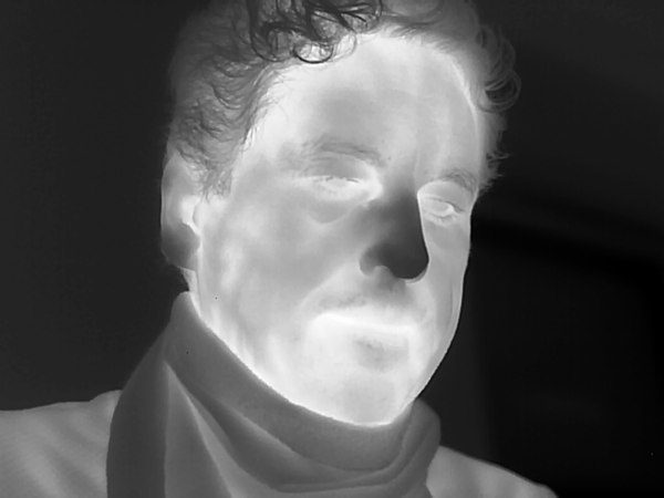
Sander Gierkink
Teledyne Dalsa, the Netherlands
Abstract
Thermal imaging is the capturing and displaying of the self-radiated energy of objects, in the Long Wave Infrared (LWIR) spectral range of 8-14µm. This is the spectral range that we perceive as “heat”. Uncooled LWIR imaging is typically based on the detection of temperature dependent resistance change of micro-bolometer pixels. A common pixel material of choice is Vanadium-Oxide, due to its large temperature coefficient of resistance (TCR). Vanadium-Oxide focal plane arrays are integrated on top of a CMOS Read-Out Integrated Circuit (ROIC) using MEMS fabrication techniques. The micro-bolometer pixels are designed for low thermal leakage towards the CMOS substrate and vacuum sealed to avoid thermal convection towards surrounding gas molecules. The CMOS ROIC integrates pixel biasing and addressing, Analog-to-Digital conversion (ADC), signal timing and digital data serialization. A typically required minimum detectable, noise equivalent temperature difference (NETD) is 50mK. This poses challenges on pixel bias and ADC design. The NETD sets a maximum limit on allowed ADC equivalent input noise. On the other hand, pixel resistance mismatch due to fabrication spread sets the minimum required ADC signal range, as ADC clipping must be avoided at all cost. Ideally, the ROIC handles a scene temperature range from NETD to 1000⁰C without any internal range setting adjustments. In this presentation, design considerations and architectures for micro-bolometer CMOS ROICs are discussed and live thermal image streams are shown.
About the author
Sander L. J. Gierkink received the M.Sc. and Ph.D. degrees in electrical engineering from the University of Twente, The Netherlands, in 1994 and 1999, respectively. In 1999, he joined Bell Laboratories, Lucent Technologies, Murray Hill, NJ, where his work focussed on RF circuit design for wireless LAN. He continued to work at Agere Systems, Allentown, PA, after it spun off from Lucent. In 2004, he joined Conexant Systems, Red Bank, NJ, where he worked on phase-locked loop and line-driver design for wire-line applications. In November 2008, he joined Axiom IC, Enschede, The Netherlands, currently part of Teledyne Dalsa, where he works on Read Out IC design for thermal focal plane imaging and new applications for imagers in medical applications.
